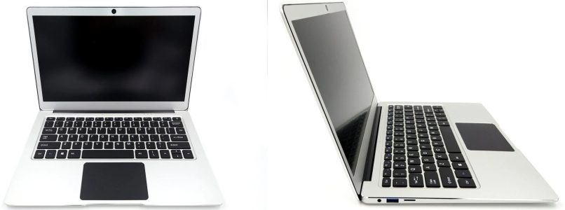
I own a Jumper EZbook. It cost about as much as a fancy dinner, it has a Celeron N3450, 6 GB of RAM, and the ambition of a tired snail. Under any sustained load its four cores sag down to about 1.5 GHz and stay there, because Intel decided this chip lives on a 6 watt diet and the firmware enforces it with religious zeal.
This is the story of how I doubled that budget to 10 W, and, more interestingly, of all the walls I ran into face-first along the way. Because the honest version of a hardware-hacking afternoon is not « I found the register. » It is « I found the wrong register, declared victory, declared defeat, declared victory again, and only then found the right one. »
The short version
The PUnit enforces PL1 = min(MMIO RAPL limit at 0x70A8, MSR RAPL limit 0x610). The firmware nails both to the fused 6 W TDP. You must raise both, and the MSR one must be locked, or the GPU will quietly undo your work.
The whole fix is two register writes at boot:
MMIO MCHBAR(0xFED10000)+0x70A8 := 0x00008f0000dd8a00   # PL1 10 W / PL2 15 W
MSR  0x610                     := 0x80008f0000dd8a00   # same, + bit 63 = LOCK
It works in every workload, GPU included: CPU-only 5.97 to 10.12 W (1.5 to 2.09 GHz), combined CPU+GPU 5.99 to 9.98 W. Peak temperature at 10 W is 84 °C against a 105 °C limit, so this was never about heat, only policy.
Show me the numbers
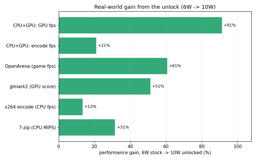
Real workloads, stock 6 W against unlocked 10 W (the full method and the 6 to 15 W sweep are in the repo’s BENCHMARKS.md, github.com/fabien0008/jumper-ezbook-power-unlock):
| Workload | 6 W (stock) | 10 W (unlocked) | Gain |
|---|---|---|---|
| OpenArena (game fps) | 69.1 | 111.0 | +61% |
| glmark2 (GPU score) | 205 | 310 | +51% |
| 7-zip (CPU MIPS) | 4858 | 6383 | +31% |
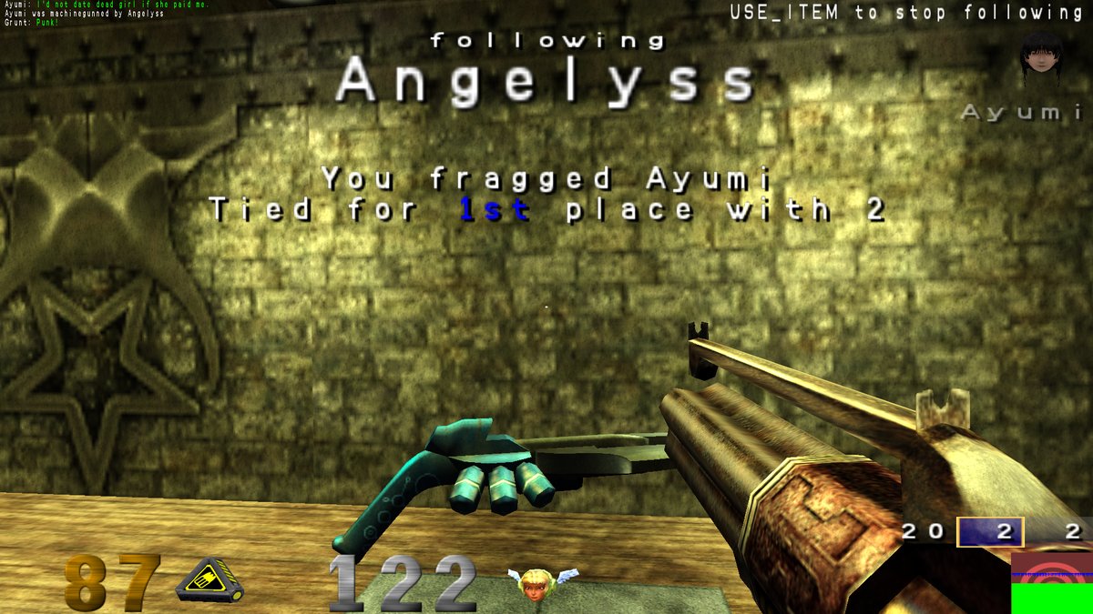
| CPU+GPU mixed (glxgears fps) | 134 | 257 | +91% |
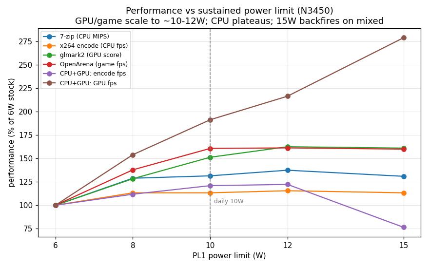
The games and the mixed loads are the big winners. The pure-CPU stuff tops out around 8 to 9 W because the all-core clock hits a hard ratio ceiling long before it runs out of watts, which is exactly why 10 W, and not more, is the sweet spot. Push to 15 W and you gain almost nothing and can even lose (more on that crime later).
The patient
Jumper EZbook, Intel Celeron N3450 (Apollo Lake / Goldmont, 4 cores, 6 W TDP), 6 GB RAM, Intel HD Graphics 500.
AMI Aptio UEFI. From earlier adventures I already knew how to read and write the SPI flash and the AMI Setup NVAR variable straight from Linux. That earlier work also taught me a brutal lesson that haunts this whole tale: a lot of the knobs the BIOS proudly exposes are dead. They sit in AMI’s template, the menu shows them, you change them, you feel powerful, and the firmware never wires them to anything. (I learned this the hard way with the DVMT graphics-memory setting, which does precisely nothing.) Remember that. It comes back.
Clocks: base 1.1 GHz, all-core burst capped at 2.1 GHz, single-core 2.2 GHz (MSR 0x1AD = 0x15151516). TjMax = 105 °C (MSR 0x1A2 = 0x690000), a detail that will matter, because it means the 6 W cap is a choice, not a thermal necessity.
The itch: make the thing hold its turbo under load instead of crawling at 1.5 GHz.
The investigation, dead ends and all
Act 1: the obvious lever. Wrong, of course
Intel documents a package power limit MSR, MSR_PKG_POWER_LIMIT (0x610). I decoded the factory value like a good citizen:
0x610 = 0x00008f0000dd8600
  PL1 (sustained) = 0x600 * (1/256 W) = 6.00 W, enabled
  PL2 (burst)     = 0xF00 * (1/256 W) = 15.00 W, enabled
  lock bit63      = 0   (not locked -> I can write it!)
Power unit confirmed via MSR 0x606 (1/256 W), the kernel’s powercap sysfs agreed, the lock bit was clear. Easy. I wrote PL1 = 10 W:
0x610 := 0x00008f0000dd8a00 # PL1 = 0xA00 = 10 WIt read back perfectly. powercap cheerfully reported 10 W. I started a load, rubbed my hands… and the package sat at 5.97 W, cores at 1.5 GHz, with the power-limit throttle flag (THERM_STATUS, 0x19C) lit up like a Christmas tree. The MSR was obeyed by everyone except the hardware. PCODE was overriding me. First wall.
Act 2: the MMIO mirror. Right idea, wrong address
On Core CPUs the limit is mirrored in MMIO at MCHBAR + 0x59A0, and the silicon enforces the lower of MSR and MMIO. This is the trick ThrottleStop and XTU use. I found MCHBAR at PCI 0:0.0 offset 0x48, base 0xFED10000, and read 0xFED159A0:
MMIO @0xFED159A0 = 0x0000000000000000Nothing. Zeros. « Ah, » I said, with all the confidence of a man about to be wrong, « there is no MMIO mirror on this chip. » Hold that thought.
Act 3: config-TDP. The chip just laughs
0x648 CONFIG_TDP_NOMINAL : #GP
0x649 CONFIG_TDP_LEVEL1  : #GP
0x64A CONFIG_TDP_LEVEL2  : #GP
0x64B CONFIG_TDP_CONTROL : #GP
Every config-TDP MSR throws a general-protection fault. Apollo Lake simply doesn’t implement the feature. Next.
Act 4: the voltage regulator. Innocent
MSR 0x601 = 0xa8, roughly 21 A of current limit, comically far above anything 6 W needs. Not the culprit.
Act 5: the BIOS knob that smells like a trap
Digging through the extracted IFR (the AMI setup form), I found this beauty:
"TDP Limit"  Help: "Turbo-XE Mode Processor TDP Limit in Watts.
             0 means using the factory-configured value."   VarOffset 0xEC
A power limit, in watts, right there in the BIOS variable store! I set NVAR offset 0xEC = 0x0A (10 W) in both redundant Setup stores, EIST and Turbo enabled, and rebooted to test, heart full of hope.
Result: 5.97 W. Nothing. The field is gated behind SuppressIf QID 0x352==0, a « Turbo-XE supported » flag that is 0 on this locked SKU, so the firmware never feeds 0xEC to the PUnit. The exact same dead-knob trap as DVMT. I should have seen it coming.
Act 6: in which I confidently surrender
So I wrote it up: the 6 W limit is PCODE-locked, unreachable by any lever. Defeat, signed and filed.
It was, of course, completely wrong, and the only reason I reopened the case is that someone refused to believe it. « I was quite sure we could do that, » they said. Annoyingly, that is exactly the kind of sentence that turns out to be right.
Act 7: reopening the one read I never trusted
The weakest link was Act 2. A register that reads as clean zeros is suspicious: real MMIO almost never does that. Two questions.
Is /dev/mem even letting me read MCHBAR? CONFIG_STRICT_DEVMEM=y, but on x86 that still allows mmap of non-RAM holes (it would fail loudly with EPERM otherwise). The read path was legit.
Is MCHBAR actually live? I scanned the whole 32 KB window: 764 non-zero dwords, real data everywhere. Very much alive. Then I searched it for the RAPL signature (the PL2 word 0x8F00):
+0x70A8 = 0x00008F0000DD8600 PL1=6.00W PL2=15.00W <-- THERE IT ISThe MMIO package-limit register on Apollo Lake lives at 0x70A8, not the Core 0x59A0. I had been reading an empty parking space three buildings over. It held the factory 6 W, untouched by my Act 1 MSR write, and this was the one the hardware actually obeys.
Act 8: the write that worked
0xFED170A8 := 0x00008F0000DD8A00 # PL1 = 10 W| Metric | Before (6 W) | After (10 W) |
|---|---|---|
| Steady-state power | 5.97 W | 10.12 W |
| All-core clock | ~1.5 GHz | 2.09 GHz |
| Package temperature | 62 °C | 76 °C |
2.09 GHz is the all-core ratio ceiling, so for pure CPU this is as good as it gets. I was a hero. For about ten minutes.
Act 9: « and does it help the GPU? » A self-inflicted wound
The first combined CPU+GPU test produced glorious nonsense: the « 10 W » run drew 14.9 W, the « 15 W » run drew 9.9 W. Lower limit, higher power? Witchcraft?
No: sampling error. I measured 8 to 18 s into the load, smack inside the ~28 s PL2 burst window, where both runs are governed by the 15 W short-term limit, not PL1. Measure PL1 and you must wait out the burst (more than 35 s). Embarrassing, fixed, moving on.
Act 10: the GPU latch reveals itself
With an honest steady-state test (4 CPU workers + fullscreen glxgears):
[PL1=10W] pkg=5.99 W  GPU=200 MHz  CPU=1195 MHz
[PL1=15W] pkg=5.99 W  GPU=200 MHz  CPU=1195 MHz
Both pinned at 6 W, CPU strangled back to 1.2 GHz, even though my 0x70A8 still read 10 W, and i915 was not secretly rewriting it (I checked before, during and after). The moment the GPU does anything, something else slams the package back to the SoC TDP. I went hunting and found suspicious read-only registers (0x7870 ≈ 6 W, 0x70A0 = TDP 6 W), no writable per-plane MSRs (0x638/0x640 both #GP)… and concluded the GPU ceiling was baked into PCODE, untouchable.
Act 11: the latch, and why your browser ruins everything
A per-second trace under pure CPU load shows the mechanism with cruel clarity:
 t      GPUmhz  CPUmhz  pkgW
 1-9     100    2089    ~10.0   GPU asleep (RC6) -> full 10 W, full turbo
 10      300    1392     6.65   GPU twitches -> package collapses
 16-30  ~100   ~1450    ~6.0    GPU asleep again... but power STAYS at 6 W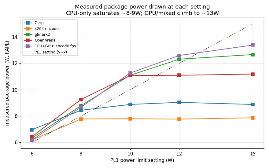
10 W holds only while the GPU is in deep sleep. The instant it wakes, to composite a window, scroll a page, blink a cursor, the package drops to 6 W and stays there, sulking, even after the GPU dozes off again. So Chrome, which keeps the iGPU permanently caffeinated, would keep me at 6 W forever. The CPU win was real only for headless, screen-idle grinding: compiling, encoding, compression.
And so, for the second time, I closed the case as unwinnable. Spoiler: it was not.
Act 12: the breakthrough hiding in coreboot
Pushed (again) to look harder, I went and read the coreboot Apollo Lake source, and there it was, stated outright in a commit message:
« This RAPL MMIO register is a physically separate instance from RAPL MSR register. The Punit algorithm constrains performance to whichever power limit is lower between both registers. » And: « FSP code sets the PL1 value as 6 W in RAPL MMIO register based on fused soc tdp value. »
PL1 = min(MMIO, MSR). Two separate registers. I had spent Act 8 onward smugly holding the MMIO at 10 W… and never once re-checking the MSR. So I looked:
during GPU load: MSR 0x610 = 0x...8600 (6 W!) MMIO = 0x...8a00 (10 W)The MSR had been reset to 6 W. The famous « GPU latch » was never some locked fortress register: it was PCODE quietly resetting the MSR copy to 6 W whenever the GPU stirs, and min(10, 6) = 6. The fortress was a sticky note.
Proof: rewriting the MSR to 10 W every second during a combined load held the package at ~10 W. But the elegant fix is the MSR’s own lock bit (63): write 10 W with bit 63 set and PCODE can no longer touch it:
MSR 0x610 := 0x80008f0000dd8a00 # PL1 10 W, PL2 15 W, LOCKEDCombined CPU+GPU load, no daemon, no babysitting:
MSR during load : 0x80008f0000dd8a00  (held!)
package         : 9.98 W   (was 5.99)
GPU             : ~383 MHz (wide awake)
CPU             : ~1.57 GHz
min(10 locked, 10) = 10, GPU or no GPU. The unlock now applies to games, video, browsing, everything. Two registers, one lock bit, and a great deal of humility.
The verdict
Enforcement is PL1 = min(MMIO at 0x70A8, MSR 0x610), so both must be raised, and the MSR must be locked or the GPU resets it.
| Lever | Writable? | Verdict |
|---|---|---|
| MMIO 0x70A8 (package limit) | yes | required: raise to 10 W (one half of the min) |
| MSR 0x610 PL1 + LOCK (bit 63) | yes | required: raise to 10 W, locked (PCODE resets it on GT activity otherwise) |
| MMIO 0x59A0 (Core offset) | n/a | wrong offset on Goldmont, the great red herring |
| MMIO 0x7870 / 0x70A0 | no | TDP/status read-outs; look like the GT limit, aren’t |
| config-TDP 0x648 to 0x64C | no | #GP, unimplemented |
| PP0/PP1 limit MSRs 0x638/0x640 | no | #GP, don’t exist |
| BIOS NVAR « TDP Limit » 0xEC | yes (flash) | not plumbed, a dead knob |
For the record, the map around the register (MCHBAR base 0xFED10000): +0x70A0 is PKG_POWER_INFO, the fused 6 W TDP, read-only; +0x70A8 is the writable PACKAGE_RAPL_LIMIT; +0x7870 is a RAPL-shaped, read-only red herring. The limit qword itself: bits [14:0] PL1 power (× 1/256 W), bit 15 PL1 enable, bit 16 clamp, bits [23:17] time window, bits [46:32] PL2, bit 47 PL2 enable, bit 63 lock.
Doing it yourself
Everything here needs root, because it pokes /dev/mem and MSRs. The fix is exactly the two writes from the short version, in that order: the 64-bit MMIO write at 0xFED170A8 (I do it from a small Python script that mmaps /dev/mem), then the locked MSR write, for which msr-tools is enough:
sudo modprobe msr
sudo wrmsr -a 0x610 0x80008f0000dd8a00
If you only write the MMIO half, you get the CPU-only boost and GPU loads still latch to 6 W. On a different board or firmware, do not reuse my addresses: scan the MCHBAR window for the RAPL signature first, the way Act 7 did.
Both registers are volatile and the lock clears on reboot, so a tiny oneshot systemd unit re-applies the fix at every boot. The complete lab notebook, every dead end included, is public: github.com/fabien0008/jumper-ezbook-power-unlock.
What the 10 W actually buys you
It raises the shared package budget. Under a combined load the CPU and GPU now split 10 W (CPU ~1.57 GHz + GPU ~383 MHz) instead of jointly suffocating at 6 W. It does not lift the per-domain ceilings: all-core CPU is still ratio-capped at 2.1 GHz, the GPU at 700 MHz, but nothing is starved any more.
Why not crank it to 15 W?
Because I tried, and measured it. Past 10 W the returns evaporate: CPU is flat (ratio-capped), glmark2 gains a measly +7% at 12 W then plateaus, the game is already maxed at 10 W, and at 15 W it actively backfires on mixed loads: with a bigger budget and no per-domain limit, the uncapped GPU gorges itself and starves the CPU encode down to worse-than-10 W numbers, all while running hottest (87 °C). More watts, less work, more heat. 10 W is the honest optimum, which is why the daily config stops there. If you insist on experimenting, PL1 = 12 W is MMIO 0x00008f0000dd8c00 and MSR 0x80008f0000dd8c00.

Before you go poking
Everything runtime is volatile: a reboot restores the factory 6 W, lock and all. The only thing that ever touched flash was the NVAR experiment, and we already established that knob is a dud.
TjMax is 105 °C; the worst I measured was 87 °C, at 15 W. Thermals were never the limit on this chassis, but if yours runs hotter, watch THERM_STATUS (MSR 0x19C) and the thermal zones.
/dev/mem pokes are a loaded gun. The wrong MCHBAR offset can hang the machine instantly. Every address here is specific to Apollo Lake (N3450).
Three buildings over, an empty parking space still reads 0x0000000000000000. Don’t trust the first clean zero you meet.